



Product Center
Current Option:All Product
-
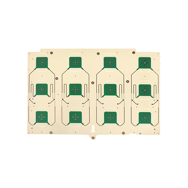
HF Antenna Boards2L
HF Antenna Boards2L
▪ Layers: 2L▪ Material: Doosan DS-7409DV▪ Board Thickness: 0.6mm ±10%▪ Min Line Width / Spacing: 0.580mm ±5%▪ Min Hole Size: 0.2mm▪ Surface Finish: Immersion Tin
More > -
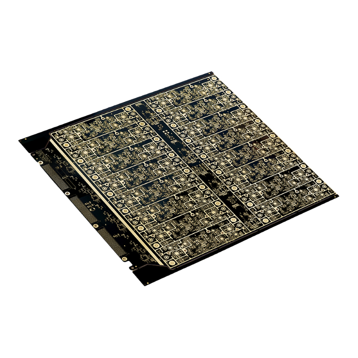
5G Active Antenna Boards22L
5G Active Antenna Boards22L
▪ Layers: 22L▪ Material: Doosan DS-7409DV HVLP▪ Lamination: 2 times lamination▪ Process: 11 sets of backdrilling tapes, VIPPO▪ Embedded with 22 copper blocks▪ 10 types of impedance (single-ended / differential)▪ High & low voltage electroplated hole filling process
More > -
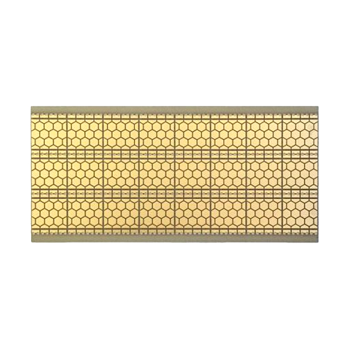
LED Ceramic Substrates2L
LED Ceramic Substrates2L
▪ Layers: 2L▪ Material: Alumina Ceramic▪ Board Thickness: 1.2mm▪ Inner & Outer Copper Thickness: 35μm▪ Surface Finish: ENEPIG
More > -
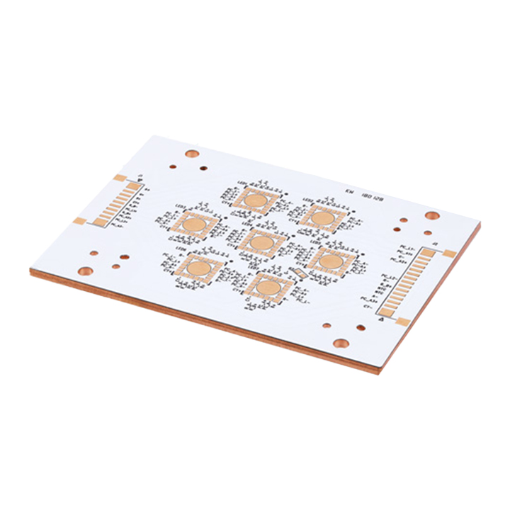
Thermal Separate Cu Boards1L
Thermal Separate Cu Boards1L
▪ Layers: 1L▪ Material: Copper Base Substrate▪ Board Thickness: 3.2mm▪ Inner & Outer Copper Thickness: 140μm▪ Surface Finish: ENEPIG
More > -
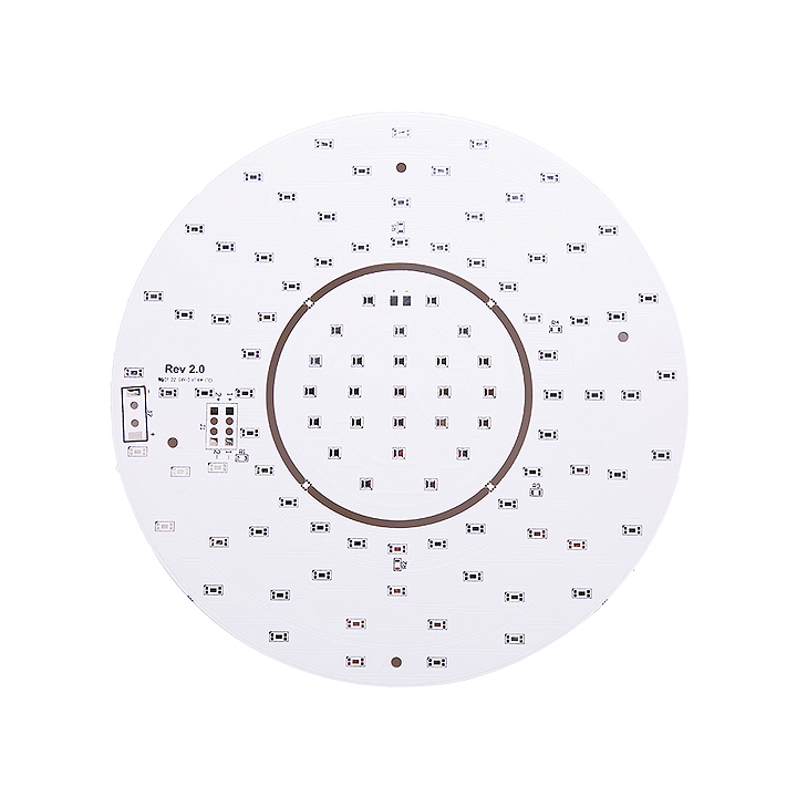
3W High Thermal Al Boards1L
3W High Thermal Al Boards1L
▪ Layers: 1L▪ Material: VT4B9▪ Board Thickness: 1.524mm▪ Inner & Outer Copper Thickness: 140μm▪ Surface Finish: HASL
More > -
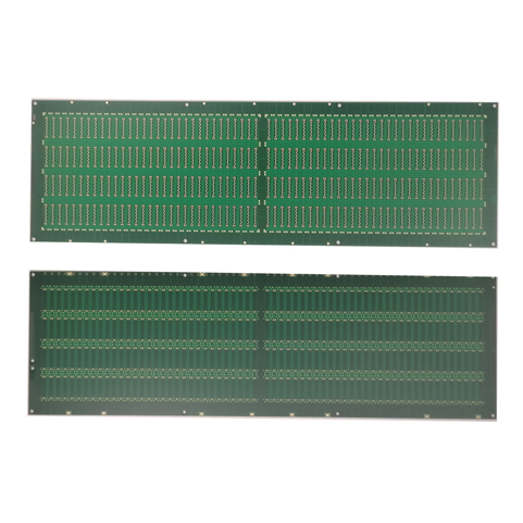
Fingerprint Modules2L
Fingerprint Modules2L
◆ Structure: 2L,Substrate thickness tolerance±15μm;Mechanical Drilling,Filled Via with SM or resin;◆ Tenting process,L/S≥35/35μm;◆ AUS320/25±7μm,SM Flatness≤7um;◆ Surface finish: Soft Ni/Au +Etch-back
More > -
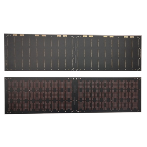
Memory Chips2L
Memory Chips2L
◆ Structure: 2L,Total thickness:100 μm min;Mechanical Drilling,Filled Via with SM;Laser Drilling,Filled Via with Copper, dimple≤5μm;◆ Tenting process,L/S≥35/35um;MSAP process,L/S≤25/25μm;◆ SM colour: Green or Black matte /thickness 20+/-7μm,SM Flatness≤7μm;◆ Surface fini...
More > -
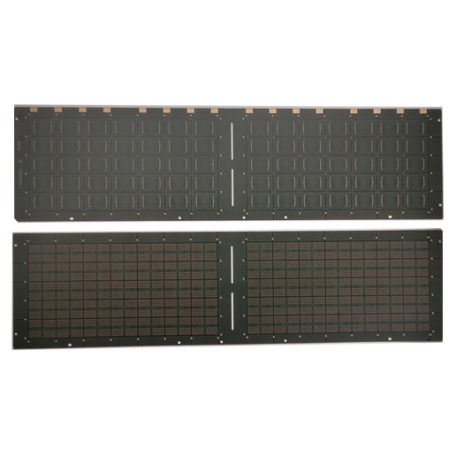
Memory Chips3L
Memory Chips3L
◆ Structure:3L Coreless, Total thickness:130μm;◆ MSAP process,BF Pitch/Width min /Space min :65/35/15μm;◆ Warpage≤2mm(before reflow);◆ Surface finish: AFOP(TOP:Ni/Au,BTM: OSP)
More > -
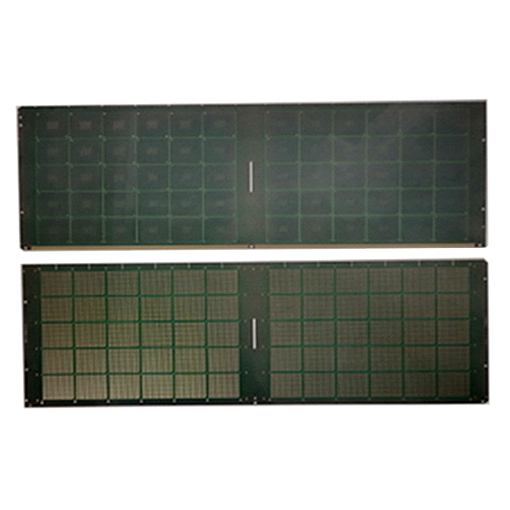
Application Baseband Chips6L, 2+2+2
Application Baseband Chips6L, 2+2+2
◆ Structure : 6L, 2+2+2,Total thickness 400 μm, core thickness 150μm;Inner layer: 75μm laser dirlled“X” hole ,copper filled. Outer layer:60μmlaser blind via.◆ Fine line: inner layerMSAP process,L/S=15/15 μm.◆ AUS SR1/thickness 15+/-7μm,SRO=105μm,SM shift tolerance≤15...
More > -
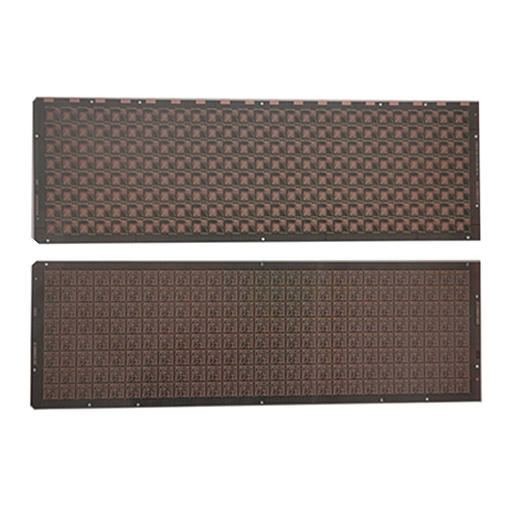
Application Baseband Chips2L
Application Baseband Chips2L
◆ Structure : 2L,Total thickness170 μm, core thickness 100μm;◆ MSAP process,L/S=20/20μm◆ 75μm laser dirlled “X” hole ,copper filled.Bonding finger Pitch: 95μm(50/40μm)BOL Pitch: 55μm(25/30μm)◆ Surface finish:Soft Ni/Au+OSP +Etch-back
More > -
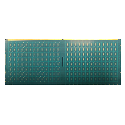
HPC12L
HPC12L
◆ Structure:12L,5+2+5◆ Core: BT / thickness 0.8mm◆ Bulid up : GX92/ thickness 25μm
More > -
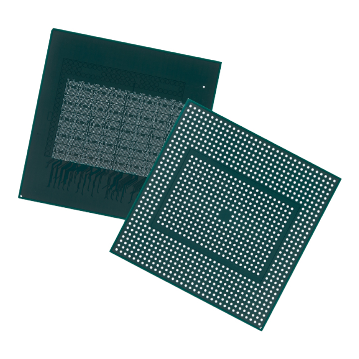
Flip Chip BGA8L
Flip Chip BGA8L
◆ Layers: 8L (3+2+3 stack-up)◆ Material: MCL-E-705G + ABF GL102◆ Board Thickness: 0.76 mm◆ Size: 50×50 mm◆ Inner & Outer Copper Thickness: 17 μm◆ Min Line Width/Spacing: 10/10 μm◆ Min Hole Size: 50 μm◆ Surface Finish: Immersion Tin + OSP
More >